Fachzeitschrift für Hochfrequenz- und Mikrowellentechnik
Aus Forschung und
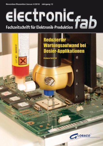
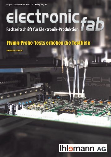
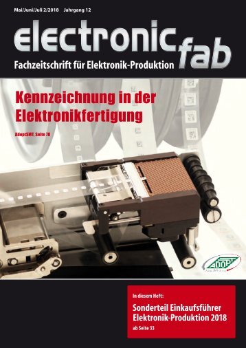
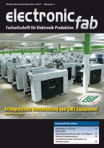
Aus Forschung und Technik World’s first multispectral time-delay-integration image sensor based on CCD-in-CMOS technology Figure 1: Schematic representation of a multispectral TDI image sensor with 7 bands At this year’s SPIE Photonics West, San Francisco, imec showcased a prototype of a high-performance multispectral time-delayintegration (TDI) imager that is based on charge-coupled device (CCD)-in-CMOS technology. Due to its high sensitivity and record high speed (up to 300 kHz), this next-generation TDI imager targets highend applications, such as remote sensing, life sciences and machine vision. The specialty imagers are offered through various business models, including full-custom design, prototype TDI sensors and evaluation cameras. TDI imaging technology relies on the collection of charges that are generated from multiple exposures of an object moving linearly with respect to the imager. Traditionally, this is done through CCD technology where the charge transfer in the CCD pixels results in a noiseless integration and transfer synchronized with the moving scene. By implementing the CCD TDI pixels together with a CMOS readout, imec combines the best of both worlds on one single chip: lownoise TDI performance, and low-power, on-chip integration of fast and complex circuitry readout. Imec produced the sensors in one CMOScompatible flow, resulting in a simple and cost-effective solution. Using backsideillumination technology, the area which is exposed to light is maximized, increasing the sensor’s light sensitivity. To enhance the TDI imaging performance, the TDI CCDin-CMOS technology was combined with multispectral or RGB color filters that can be processed at wafer level or alternatively, filters on glass may be used. Imec offers its CCD-in-CMOS TDI technology through various business models, ranging from full-custom design to offering Figure 2: Packaged prototype of a multispectral TDI image sensor with 7 Bands of imec’s prototype TDI sensors and evaluation cameras. The prototype TDI sensors use a format with 4,096 columns and 256 stages per CCD array (or band). A version with one CCD array is available, as well as a 7-band version, allowing to add 7 spectral filters. The prototypes integrate CMOS drivers and readout circuitry. ■ Imec www.imec-int.com Imec, Holst Centre and Cartamundi introduce plastic Near Field Communication Tag communicating with Smartphones At the 2017 International Solid-State Circuits Conference in San Francisco, imec and Cartamundi demonstrated a world first thin-film-tag on plastic, compatible with the near field communication (NFC) Barcode protocol, a subset of ISO14443- A, which is available as standard in many commercial smartphones. The innovative NFC tag is manufactured in a thin-film transistor technology using indium gallium zinc oxide thin-film transistors (IGZO TFT) on a plastic substrate. Plastic electronics offers an appealing vision of low-cost smart electronic devices in applications where silicon chips were never imagined before. Item-level identification, smart food packaging, brand protection and electronic paper are just a few examples. Such new applications will require a continuous supply of countless disposable devices. Imec’s IGZO TFT technology uses large-area manufacturing processes that allow for inexpensive production in large quantities - an ideal technology for ubiquitous electronic devices in the Internet-of-Everything. “Making a plastic electronics device compatible to the ISO standard originally designed for silicon CMOS was a very challenging research and development expedition” stated Kris Myny, senior researcher at imec. “Our collaboration with Cartamundi enabled us to develop a truly industry-relevant solution”. The researchers developed a self-aligned TFT architecture with scaled devices optimized for low parasitic capacitance and high cut-off frequency. This allowed design of a clock division circuit to convert incoming 13,56 MHz carrier frequency into system clock of the plastic chip. Optimizations at logic gate and system level reduced power consumption down to 7.5 mW, enabling readout by commercial smartphones. The results were presented in paper 15.2: “A Flexible ISO14443-A Compliant 7.5 mW 128b Metal-Oxide NFC Barcode Tag with Direct Clock Division Circuit from 3.56MHz Carrier” K. Myny, Y.-C Lai, N. Papadopoulos, F. De Roose, M. Ameys, M. Willegems, S. Smout, S. Steudel, W. Dehaene, J. Genoe, Feb. 7, 2017 ■ Imec www.imec-int.com 6 hf-praxis 5/2017